 |
 |
||
Integrated Optofluidics: Manipulation and Analysis of Single Molecules on a Chip Optofluidics is a rapidly emerging area of research that can be described as “The combination of both integrated optical and fluidic components in the same miniaturized system”. Optofluidics holds great promise for novel devices for biomedical instrumentation, analytical chemistry and other fields that deal with liquid analytes. For more details on the fundamentals and recent trends in this emerging field, please see our book [1] and a couple of review articles in the dedicated focus issue on optofluidics in Nature Photonics [2-4]. | ||
| ||
|
A major thrust in the field is to use integrated optics to replace the bulky microscopy analysis that is still commonly in use. This will enable a fully planar, fully integrated lab-on-a-chip on which optical signal, electronics, and fluids run in the plane of the chip. The Applied Optics group has led the field of planar integrated optofluidics with the development of liquid-core ARROW waveguides that allow for using integrated optics technology in conjunction with microfluidics. The W.M. Keck Center for Nanoscale Optofluidics was established in 2009 at UCSC has further helped catalyze interdisciplinary research that advances and uses waveguide-based chips. Our research emphases include:
|
||
|
Particle detection and analysis | ||
|
Fig. 1 shows cross sections of micron-scale liquid core waveguides that use dielectric multilayers to confine light in the hollow channel. Fabrication is fully compatible with silicon processing technology and developed by our collaborators, the Micro-Technologies Group of Aaron Hawkins at Brigham Young University. The use of small cross sections is a key requirement for creating the small optical excitation volumes that are necessary to achieve single molecule detection. | ||
| ||
Fig. 1: SEM images of typical solid- and hollow-core ARROW waveguides used to construct optofluidic platform. Fig. 2 shows a schematic of the optofluidic principle. Molecules are moved electrokinetically or with pressure through a liquid-core ARROW. They are optically excited via an intersecting solid-core waveguide. Emitted light is collected by the LC-ARROW in the plane of the chip and guided to the chip edge after being coupled to another solid-core waveguide. Also shown is a trace of fluorescence bursts from single liposomes that are passing the waveguide intersection. The signal can be analyzed with various methods to yield information about the concentration and properties of the detected biomolecule. Similar measurements have now been demonstrated on viruses (Q-beta bacteriophages), again resulting in single particle sensitivity via FCS [6]. | ||
|
| ||
|
Fig. 2: Optofluidic chip for single particle analysis. Solid- and liquid-core ARROWs intersect on the chip, defining a small optical excitation volume. Particles are added to fluidic reservoirs and driven by the excitation spot, creating characteristic signals. We are currently pursuing several future directions, most notably new types of optical waveguides, implementation of advanced optical detection techniques, addition of electrical and optical control of single biomolecule, analysis of RNA translation in single ribosomes. The detection of biomarkers for infectious diseases and cancer is a particular focus of our lab (see, for example, this link to our work on detecting single viral nucleic acids which was selected as a conference highlight at CLEO 2013). |
||
| Particle manipulation | ||
|
It is well known that momentum transfer from photons onto solid objects result in optical forces. These can be used to optically manipulate micro- and nanoscale particles, the best-known example being the laser tweezers that are routinely being used in cell biology and other fields. We are studying optofluidic implementations of optical forces using liquid-core waveguides. One example is the use of optical particle manipulation for waveguide characterization [7]. Fig. 3 shows a microbead propelled through a liquid-core waveguide channel by the scattering force that the optical mode exerts on it. The force is proportional to the power at any given particle position, determining the velocity as the particle moves along. Thus, the waveguide loss which reduces the available power can be extracted by recording the particle’s position as it moves along the channel (see Fig. 3). If the particle position is also tracked laterally, the lateral mode structure can be extracted from the particle histogram (Fig. 3). These measurements show that optical particle manipulation can be used as a simple, rapid, and non-destructive means for hollow-core waveguide characterization. |
||
 |
||
Fig. 3: Waveguide characterization using optical forces. Top left: time-dependent position of an optically propelled microbead; bottom left: time-dependent particle position along waveguide channel; right: histogram of lateral position and match with waveguide mode calculations. A second example for the use of optical forces for particle manipulation is the development of a novel all-optical dual beam trap [8,9]. The concept is shown in Fig. 4. Two counterpropagating beams are sent through the waveguide. Unlike a conventional dual beam trap, the scattering force exerted by the two beams is asymmetric because of the presence of waveguide loss which results in an asymmetry in power distribution. At one point along the waveguide, the longitudinal forces are equal and a particle can be trapped. The figure also shows a microscope image of two simultaneously and independently trapped microbeads, one using the new loss-based dual beam trap and one using a more traditional dual beam trap (see [8] for details). The trapping architecture is compatible with simultaneous fluorescence detection of the trapped objects and has enabled us to carry out prolonged interrogations of microbeads and E.coli bacteria. |
||
 |
||
Fig. 4: Loss-based all-optical dual beam trap. Left: schematic of applied beams; right: microscope image of two microbeads trapped in planar, on-chip trap. The scattering forces responsible for creating the trapping potential act along the entire waveguide channel. Thus, if multiple particles are present, they are all subject to these optical forces and can be driven towards a single trapping location. This concept can be used to create an all-optical particle concentrator which enhances the particle concentration locally at a desired point [9]. This concept is shown in Fig. 5 which shows a large increase in fluorescence signal as >100 fluorescent microbeads are optically accumulated and trapped in the waveguide intersection. |
||
 |
||
Fig. 5: Optofluidic particle concentrator (a) Concentrated 1µm particles at a waveguide intersection. (b) A particle ensemble transported to the far end of the hollow waveguide through the application of an additional electric field. (c) Temporal evolution of the fluorescence signal during the optical concentration of 500nm particles. Insets show fluorescence snapshots of a single particle and the final particle ensemble. |
||
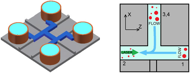
Optical particle sorting is another application of optical forces on a chip. Recently, we have demonstrated optical particle sorting in various geometries on an optofluidic chip with an H-shaped channel layout as shown in Fig. 6 [12]. Optical and drag forces scale differently with size. Therefore, a combination of pressure-based flow and optical beams in the liquid-core channel can be used to selectively remove particles from the channel. Fig. 6 shows one geometry in which the optical beam directly opposes pressure-based flow. Large particles are pushed along the optical beam direction, while small particles remain in the flow. Particle separation can be accomplished with 100% sorting efficiency in this case. | ||
|
| ||
Fig. 6: Chip layout for optofluidic particle sorting. An optical beam counteracting pressure-based flow selectively removes large particle from a mixture. [12] | ||
|
Hybrid integration | ||
|
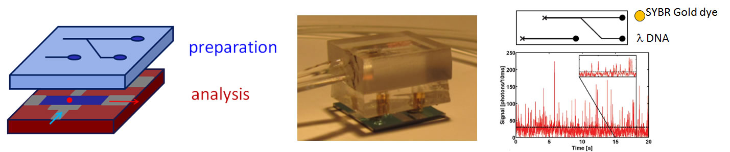
One of the original visions for the field of optofluidics was to create chip-scale systems with sections optimized for different purposes [1]. We have recently reported the first demonstration of a vertically integrated device, consisting of a PDMS-based microfluidic layer on top of the silicon-based ARROW chip [13]. This arrangement allows for separate optimization of each layer for their dedicated function. We used this device to combine canonical sample preparation elements (mixing, sorting, distribution) with single molecule optical detection sensitivity (see Fig. 7). We are working on more complex and powerful implementations that take the optofluidic approach towards a complete front-to-back analysis system for biological and chemical samples. | ||
|
| ||
|
Fig. 7: Left: Hybrid vertical integration of dedicated layers for sample processing and optical sensing; Center: reconfigurable implementation combining ARROW chip and PDMS layer; Right: Example of fluorescent labeling in PDMS layer, followed by single DNA detection on ARROW chip [13]. This work has been funded by the National Institute of Health (NIH/NIBIB, NIH/NIAID), the W.M. Keck Foundation, the National Academy of Sciences, the National Science Foundation (NSF), the Santa Cruz Cancer Benefit Group, the Rodgers Family Foundation, and the NASA University Affiliated Research Center. We collaborate with the groups of David Deamer (Biomolecular Engineering, UCSC), Harry Noller (Molecular Biology, UCSC), Jin Zhang (Chemistry, UCSC), Richard Mathies (Chemistry, UC Berkeley), Jean Patterson (TBRI), and Aaron Hawkins (BYU). [1] A. R. Hawkins and H. Schmidt (Eds.), “Handbook of Optofluidics”, CRC Press, 2010. ISBN 9781420093544. |


 |
 |

|
 |
 |
 |
 |
 |
 |
 |


Home / / / / / / Electrical Engineering Baskin School of Engineering UC Santa Cruz
© 2008 H. Schmidt. All rights reserved. Contact
 |