 |
 |
 |
 |
 |
 |
 |
 |
 |
 |

|


Home / / / / / / Electrical Engineering Baskin School of Engineering UC Santa Cruz
© 2010 H. Schmidt. All rights reserved. Contact
 |
|
Integrated Nanopores:
Nanoscopic openings in membranes have been used in single molecule analysis for some time. Typically, changes in ionic current through the pore that are caused by a particle that is moving through and obstructing the opening are detected. This principle is shown in Fig. 1: | |
|
| |
|
Fig. 1: (a) Current blockade principle of a nanopore sensor. (b) Examples of biological (left) and solid-state (right) nanopore. Initially, biological nanopores (a-hemolysin) were used to create blockade signals from single-stranded DNA molecules and have pointed a way towards rapid sequencing of DNA [1]. More recently, nanofabrication methods have been developed to place nanopores in inorganic materials, most commonly silicon nitride membranes [2]. The inherent advantages of artifical pores include robustness and flexibility in size etc.
We are interested in integrating nanopores as "smart gates" to create multi-functional optofluidic devices for single biomolecule detection and analysis. Our group is pursuing a number of research directions in this context:
Here is an overview of some of our recent results: Nanopore integration on optofluidic chip In collaboration with the Hawkins group at BYU, we developed a two-step fabrication process for defining nanopores in microfluidic, and specifically ARROW channels [3] (Fig. 2a). First, a micro-scale opening is defined with a dry etch process. This etch is terminated on top of the first ~100nm thick ARROW cladding layer. Subsequently, the nanopore is milled with a focused ion beam in our dedicated nanofabrication facility in the W.M. Keck Center for Nanoscale Optofluidics. Fig. 2b shows a 2μm micropore with a 150nm nanopore. Fig. 2c shows how the aperture size of the nanopore is modified by repeated scanning with a defocused ion beam until the pore diameter has been shrunk to 20nm. | |
|
| |
|
Fig. 2: (a) Cross-section of micropore/nanopore integration on the liquid-core waveguide. (b) Top-down view of a 150nm nanopore in a 2μm micropore. (c) Nanopore sculpting by repeated scanning with focused ion beam. Influence of 3D nanopore shape and composition on current blockades We have also shown how the nanopore signal depends not only on the size of the limiting aperture, but also on the fabrication method, resulting in different three-dimensional shapes [4]. We investigated this correlation by defining nanopores of 50nm aperture in three different ways: direct milling (DM), ion-beam (IB) and electron-beam (EB) assisted shrinking [11]. Fig. 3a shows the characteristics of an EB-shrunk nanopore. The cross-section (bottom) reveals an increase in the membrane thickness due to deposition of hydrocarbons in the vacuum chamber. This is confirmed by X-ray spectroscopy (top, center). The resulting current blockades (top, right) can be simulated very well once the 3D shape is known. Fig. 3b shows the distribution of blockade depth and duration for the three pore types. Clear differences are observed despite their nominally identical aperture size. Again, these differences are fully reproduced by taking into account the full 3D shape of the pore. | |
|
| |
|
Fig. 3: (a) Characterization of a 50nm wide nanopore shrunk to size with an electron beam. Top left: top-down view of the nanopore. Top middle: EDS spectrum of the nanopore showing carbon accumulation around the pore. Top right: comparison between experimental (symbols) and simulated (line) current blockades. Bottom: cross-section photo of the nanopore. (b) The distribution of blockade amplitude and duration for three pore types. Electrical detection of single ribosomes on a chip We first demonstrated electrical sensing of single biomolecules with a nanopore in an optofluidic devices in 2011 [6]. A nanopore (40nm aperture) was defined in an ARROW chip using ion-beam assisted shrinking. The chip layout is shown in Fig. 4a along with a photograph of a nanopore-ARROW device (inset). A solution containing 50S ribosomal subunits was introduced into the fluid reservoir on top of the nanopore, and a voltage was applied to move the ribosomes into the fluidic channel in single file. The observed electrical signal for different applied voltages is shown in Fig. 4b (inset: characteristic blockade signal caused by a single ribosome). Blockades of ~4% of the total ionic current were well resolved, with the translocation rate depending strongly on the applied potential (Fig. 4c). This strong dependence can be used in future devices for additional control. | |
|
| |
|
Fig. 4: (a) Placement of nanopore on the ARROW chip. Inset: A photo of a nanopore-ARROW chip. (b) Current blockades from individual 50S ribosomal subunits for different applied voltages. (c) Voltage dependent capture rate of single ribosomes. Correlated electro-optical detection of single biomolecules on a gated nanopore chip The full potential of the electro-optofluidic integration with an ARROW chip is only realized if the nanopore gate is combined with the optical single molecule detection capability discussed above. We demonstrated this dual-mode single molecule analysis for the first time on an optically and fluidically integrated chip [5]. Fig. 5a shows correlated electrical and optical signals created by a mixture of fluorescent nanobeads of different diameter (100 and 200nm) that were drawn through a 250nm wide nanopore. Both modalities show clean signatures from individual nanoparticles with high signal-to-noise ratio. The temporal correlation is quantified feature by the cross-correlation function between optical and electrical traces (Fig. 5b) which shows a single peak that allows for immediate extraction of the flow speed in the ARROW channel (this delay corresponds to the time it takes the nanobeads to travel from the nanopore gate to the optical excitation spot). Fig. 5c shows a scatter plot of the electrical blockade signals. The bead subpopulations are clearly resolved as the larger particles obstruct the pore more completely and produce a larger blockade amplitude. This allows us to assign each optical peak with its corresponding electrical signal and create a histogram of the optical brightness distribution for the two particle types (Fig. 5d). While the larger beads are brighter on average, there is an overlap region in which the optical signal amplitude alone is not sufficient to decide what particle created it. With the help of the nanopore gate, we can analyze the optical signal distributions and identify correlations with the particle location within the channel. | |
|
| |
|
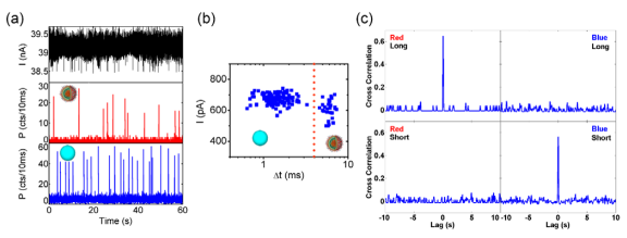
Fig. 5: (a) Correlated electrical (black) and optical (red) signals. (b) Cross-correlation function between electrical and optical signals. (c) Blockade amplitude versus duration of electrical signals. (d) Histogram of the optical brightness distribution for each particle type. We also investigated a mixture of 100nm fluorescent beads and ~100nm large influenza (H1N1) viruses using a ~150nm wide integrated nanopore. The viruses were labeled to fluoresce in the red (~670nm) while the bead fluorescence is in the blue. The resulting electrical and (spectrally resolved) optical signatures for this mixture are shown in Fig. 6a. Again, clear blockades and optical spikes are resolved, representing the first demonstration of detection of single virus particles using two modalities on a single chip. Moreover, we can now unambiguously prove the single particle nature of the optical detection as each particle has to transverse the nanopore in single file. The blockade amplitudes are quite uniform for all electrical signals (Fig. 6b) due to the similar size of the particles used. However, the events seem to separate into particle type by blockade duration as indicated by the dashed line. The optical signal allows us to prove this conjecture by computing the cross-correlations of all combinations of red/blue optical
channels with short/long blockade durations. Fig. 6c shows only two non-zero correlations, proving that all long (short) blockades are caused by viruses (beads). Fig. 6: (a) Electrical (black) and optical (red and blue) signals created by mixture of viruses and 100nm nanoparticles. (b) Blockade amplitude versus duration of electrical signals. (c) Cross-correlation functions between different electrical and optical traces. Red: optical signal of virus. Blue: optical signal of 100nm nanoparticles. Long: electrical signal with longer duration. Short: electrical signal with shorter duration. This work has been funded by the National Institute of Health (NIH/NIBIB, NIH/NHGRI), the W.M. Keck Foundation, the National Science Foundation (NSF), and the NASA University Affiliated Research Center. We collaborate with the groups of David Deamer (Biomolecular Engineering, UCSC), Harry Noller (Molecular Biology, UCSC), Jin Zhang (Chemistry, UCSC), Bill Dunbar (CE, UCSC), and Aaron Hawkins (BYU).
[1] B. M. Venkatesan and R. Bashir, “Nanopore sensors for nucleic acid analysis,” Nat. Nanotechnol., vol. 6, no. 10, pp. 615–624, Oct. 2011.
|


 |